Brett J Hamilton – Applied Research Institute, Bloomington IN.
email: brett.hamilton@theari.us
Abstract
Since the first integrated circuit (IC) was assembled from a handful of transistors, the sophistication of electronic design automation (EDA) tools has steadily increased. To date the changes have been linear and predictable, but the industry is on the precipice of a paradigm shift in the very nature of integrated circuit design. Envision complex artificial intelligence (AI) based design tools in which a human defines end user function at the highest possible level of abstraction. The AI engine freely selects design elements from vast libraries of available intellectual property (IP), or creates entirely new IP using standard cell libraries, integrating the design, likely in ways beyond human comprehension! Of great concern in such a scenario is the security/integrity of the final design, which is also tied to explainability and governability. Might an independent AI engine be applied to the completed design to ensure integrity? Are we in the early stages of an AI arms race where Nation States maneuver for advantage in the merging areas of connectivity (IoT, social media), big data, AI and powerful computer hardware? This paper will examine just such a scenario narrowly focused on the design process for microelectronic ICs that are crucial to Department of Defense (DoD) Weapon and Cyber Systems.
[Keywords: Microelectronics Integrity, AI for EDA Tools, Hardware Security, Neural Networks, Responsible AI]
Introduction
Modern Weapon and Cyber systems are extremely sophisticated, relying on state-of-the-art (SOTA) microelectronics to achieve performance only dreamed of just a few years ago. A very high percentage of the microelectronics utilized in these systems are commercial-off-the-shelf (COTS) products, many of which are designed, manufactured, packaged and tested completely outside DoD’s purview. The robustness of these COTS microelectronic products is absolutely essential to the DoD and to the warfighter.
Microelectronic hardware provides the “root-of-trust” for many DoD weapon and cyber systems. It is critical that this hardware be both trustworthy and reliable to perform as designed. Microelectronics are pervasive, for example it is estimated that there are roughly 1,000 chips in a non-electric vehicle and twice as many in an electric vehicle, many of which perform safety critical functions such as anti-lock braking and airbag deployment. In 2020 these electronics and accompanying software represented 40 percent of a vehicle’s cost. Many segments of the US economy require robust and secure interconnectivity, where again hardware often provides the “root-oftrust”. Secure communications are critical for industries such as banking, utility production and distribution, and commerce, due to reliance on an expansive internet connectivity.
IC Complexity and The Reality Of A Global IC Industry For DoD
The ability to verify the integrity of microelectronics is at the very core of a “Hardware Root-of-Trust”. For example, the Smartcard chips which are integrated into credit cards must be trustworthy and secure in their operation, otherwise public trust is lost. As design complexity and the level of integration grows, this poses a great challenge in our ability verify integrity, or even define a verifiability set of rules that could be applied. IC design has transitioned from a single individual, who completely understood every function being executed within the design, to a small team where the team leader still had a pretty good understanding of the overall design, to large diverse design teams where no single individual has visibility and understanding of the full design details. It is not unusual for over 5,000 designers to be involved in creating today’s state-of-the-art (SOTA) ICs. This contrast between the first IC and a modern IC is illustrated in figure 1.
In the early days of ICs the US government was the primary customer, driving the technology development. Miniaturization from vacuum tube technology was necessary to support the Apollo missions and the DoD immediately recognized the importance for weapon systems. In fact, one of the first customers for the newly developed IC was the US Air Force. Today the DoD represents roughly 1 percent of global IC sales, and the commercial sector is now the primary technology driver. This has forced DoD to depend upon ICs in which the design and manufacturing process flow is outside of government control.
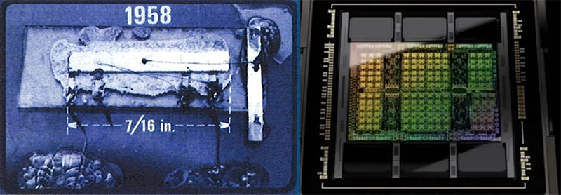
Figure 1. Left Image: Jack Kilby’s original integrated circuit contained 5 transistors. Newly employed by Texas Instruments, Kilby recorded his initial ideas concerning the integrated circuit in July 1958, successfully demonstrating the first working integrated example on 12 September 19 58. Right Image: 80 billion transistor Nvidia Hopper H100 GPU – Nvidia’s new flagship GPU for data center AI and scientific workloads (Source: Nvidia).
The International Roadmap for Devices and Systems (IRDS) looks at semiconductor foundry progression, such as the adoption of extreme ultraviolet lithography (EUV) lithography to satisfy the exploding computational demand for modern applications such as artificial intelligence (AI), high performance computing (HPC), internet of things (IoT), and 5G/6G. As we enter the Angstrom era, manufacturing complexities and costs are moving the industry to heterogeneous integration of chiplets into multi-chip packages (MCP). Today’s semiconductor chips may have as many as 80 billion transistors, but an advanced MCP device can provide a staggering 300B transistors in a single package (Figure 2). This has led to extremely complex chips and MCP’s containing 100’s of billions of individual transistors, where compute and memory are tightly coupled to reduce power. This extreme complexity coupled with lack of detailed design intellectual property (IP) insight makes independent integrity and reliability verification very challenging. As we are poised to move into the realm of AI “aided” design, the problem of circuit understanding/verification will become much more difficult, and we could certainly reach a point where it is practically impossible.
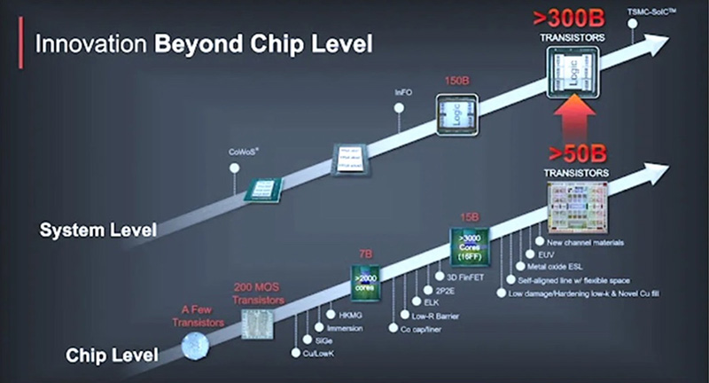
Figure 2. The bottom graph shows “Moore’s Law” progression at the chip level with the top graph showing the progression of packaging technologies.
Is AI On The Cusp Of A Capability Explosion?
Historically AI has not delivered promised advancements, but nearly a decade ago many experts in the field believed major breakthroughs were near. Cheap parallel computation, access to large data sets, and better algorithms have been identified as major factors in this supporting the belief that this breakthrough is near. While there are many factors which may contribute, three technical advancements are significant enabling factors;
- Microelectronics hardware density is approaching that of the human brain. The estimated number of Neurons in the brain is between 80B and 200B (depending on whom you ask). While there are now individual ICs with 80B transistors, the complexity of synapse connections does not directly correlate to transistor count. However, many such ICs can easily be packaged together (fig 3), and otherwise interconnected allowing virtually unlimited scaling!
- There are efforts to mimic human brain function for AI implementation. A major obstacle in AI is how to teach an AI system to learn. That has proven very difficult to implement using traditional computer programing methods. Geoff Hinton dubbed a new family of algorithms as “deep learning” to be an essential component of an AI system. A silicon-based AI system only needs to mimic the brain’s processes, not emulate them, after all airplanes don’t flap their wings, but can fly faster than a bird! Neuromorphic engineering, also known as neuromorphic computing is a concept developed by Carver Mead in the late 1980s, describing the use of very large-scale integration (VLSI) systems containing electronic analog circuits to mimic neuro-biological architectures present in the nervous system. This is but one such example of ongoing work in the field of Al.
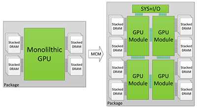
Figure 3. Package-level integration of multiple GPU modules to build larger logical GPUs can enable continuous performance scaling beyond Moore’s law. - Commercial companies such as Google and Microsoft are embracing this technology. While recent media attention has focused on large language models (LLMs), such as ChatGPT and Bard, many specialized, more narrowly focused applications such as EDA tools and manufacturing optimization (real-time yield learning) applications are marching forward. Given these recent developments, there is great interest in more energy efficient (and affordable) hardware for training and inferencing, which will include the development of more efficient algorithms. Challenges for adopting AI for Microelectronics compared to LLM includes; 1) lack of huge volumes of industry-wide training data, 2) complexity of circuit sizes attributed to Moore’s law and 3) various design technologies/styles.
What Is the Problem’s Relevance To The Existing Design Automation Tools And Methods?
How can security and integrity be rules defined and implemented? While there are a few very narrowly focused tools that address specific integrity/security issues, there is currently a void in our ability to perform this function in general terms. Thus, this is an area ripe for the application of AI methods.
AI is being aggressively applied to EDA tools by all the major vendors as exemplified in recent press releases. For example, on March 29, 2023 (Reuters) – “Synopsys Inc on Wednesday rolled out new artificial intelligence tools designed to get better results faster in the various stages of designing computing chips……Synopsys is in a race with Cadence Design Systems, its largest competitor, to add AI to chip design software.” Examples include Synopsys DSO.ai and Cadence Cerebrus.
Security centric design tools are needed to complement existing tools. The stuck-at fault model approach for test insertion is a mainstay, as it is a simple concept that is manageable using rules-based algorithms. Not to trivialize today’s tools, given optimization requirements, timing and power constraints they are very complicated. The question is, can an analogy to performance/functionality-based tools be developed for security and integrity?
Traditional design automation tool developers will likely continue to be vital participants in future AI-based development teams due to their historical understanding of the design world and widespread use by designers. However, the true power of an AI-based tool is that it will also draw knowledge from a much more diverse community of skills with expertise in hardware security, hardware/firmware hacking, Al/cognitive thinking, system design, computer science, semiconductor physics, IC design, IC design tool function, and others.
Consider the following analogy: A security weakness is detected in an IC, a “diseased circuit”. The malignant circuit is identified by the AI engine, which dispatches “digital antibodies” to destroy or repair the faulty circuit. Might a digital blueprint of basic logic cell’s function be analogous to the human genome? Mapping such logic cells to higher level of function for the purpose of identifying and targeting a “digital cancer cell” will certainly prove very challenging, just as it is with cancer. Figure 4 shows the relationship between biological and silicon with respect to schizophrenic human behavior, as AI’s hallucination problems is well known. Industry currently uses engineering change order (ECO) or change order (CO) to address bugs found later in design cycle, which is a mostly manually process.
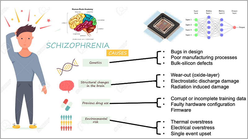
Figure 4. What I Worry About – Reliability & Robustness, “Schizophrenic – “Behaving as if one has more than one personality: wildly changeable”. Much has been written about AI’s “hallucination” problem, but it’s unclear how that might be manifested in narrowly focused AI applications such as related to IC design.
Hardware Integrity Verification Is Hard!
At leading edge foundry process nodes, currently 3-4nm in production with sub 2nm on the horizon (containing up to 80B transistors), postproduction integrity verification is an extremely difficult problem. The challenge will only get harder as the industry moves to gate-all-around (GAA) and backside power delivery. So, it becomes not just critical, but absolutely necessary to do as much verification as possible at the design phase when the entire design is in digital form, this is also the stage in which the design is the most vulnerable.
Verification of the manufactured IC can be addressed in three ways, 1) Functional Indirect, 2) Functional Direct, and 3) Physically. The level of insight, invasiveness and destructiveness varies greatly between the three categories of techniques.
Functional indirect (fig. 5) techniques apply inputs and evaluates the resultant outputs. This is often referred to as “black box” approach because generally the details of the actual operations used to generate the outputs are not known. As IC complexity has grown, such as with system-on-a-chip (SoC)s that can contain 10’s if not 100’s of separate IP blocks, this technique is not feasible. It is used for specialized cases such as “scan test”, but in that case the device is placed in a special test mode and the inputs with accompanying outputs are generated during IC design test insertion using EDA tools optimized for this purpose. Test equipment and test time can be very expensive for exhaustive testing. AI can identify a reduced number of reliable test vectors and cut-down the search space; instead of verifying with all 2^n combinations (which can theoretically take exponential time).

Figure 5. Functional indirect is providing external stimulus and recording the results. It provides limited information on the internal mechanisms at play in processing the input and generation of the output.
Functional direct allows non-destructive direct transistor operation observation based on input stimulus. Techniques utilizing scanning optical microscopes (SOM), including techniques such as laser-scanned imaging (LSI), laser voltage imaging (LVI), laser voltage probing (LVP), photon emission microscopy (PEM), and laser-assisted device alterations (LADA) are typical methods in failure analysis. They do require optical access to the backside silicon, and often require thinning for use of a solid immersion lens (SIL) to get the required magnification. These techniques are slow, and do not scale for whole chip verification. In addition, sub 10nm processes push the resolution and backside power routing prevent backside access.

Figure 6. Functional direct allows direct observation of internal activity. The image on the left is positron emission tomography (PET), a technique that uses radiation to show activity within the body on a cellular level. The image on the right is laser voltage imaging (LVI) showing circuit activity at a given clock frequency within an IC.
Physical analysis generally requires the destruction of the sample and is often used to determine the root cause of a failure once isolated using techniques such as SOM. Focused ion beams cut away a section of the chip as seen in figure 7 (right image). Sometime a thin (<300nm thick) section is removed for inspection in a transmission electron microscope (TEM) where extremely high magnification (up to 50 million times) can be achieved. TEM instruments have multiple operating modes including conventional imaging, scanning TEM imaging (STEM), diffraction, spectroscopy, and combinations of these.
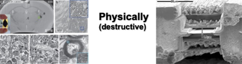
Figure 7. Physical analysis is very narrowly focused but provides the most detailed information on the physical construction such as structures and materials. The development of methods for imaging large contiguous volumes with the electron microscope could allow the complete mapping of a whole mouse brain at the single-axon level (left image). The right image is of a 300nm thick IC lamella that was prepared using a FIB.
What Does This Mean To The DoD?
In the current era of persistent cyber threat, our adversaries are extracting system level design details in digital format that could readily be utilized to guide AI systems in the insertion of hidden functions. – “Computer hackers, apparently working as spies, have stolen several terabytes of data related to design and electronics systems at the heart of the Defense Department’s massively expensive Joint Strike Fighter program.” This threat doesn’t apply to just leading-edge process nodes, in fact reproduced legacy parts would be an easier target!
How can AI help DoD with existing COTS products required to support both modernization and legacy systems?
- AI can generate advanced and dynamic encryption circuits that can be plugged-in to existing COTS products.
- Generative adversarial network (GAN) techniques can create a more intelligent and robust circuit by competing with itself.
- AI can be used to detect and classify fake and malicious hardware by identifying certain patterns/features through the analyze the fusion of multiple modalities for determining a unique microelectronic device signature (Apparatus and Method for Integrated Circuit Forensics and Testing Apparatus for Detecting Counterfeit or Defective Microelectronic Devices).
There is also the possibility for adversarial intervention, be it training data or tool design manipulation, data theft or direct insider tampering that must be considered.
There are many visionaries, including the late Stephen Hawking and Steve Wozniak who feel that AI is an extremely dangerous technology.
Let’s take a closer look at possible scenarios for the usage of advanced AI in the design of integrated circuits as an example:
- The US establishes itself as the leader in this technology and applies it to ensure the Microelectronics used in DoD Weapon and Cyber Systems are trustworthy and reliable. Safeguards are applied to the AI systems to maintain control of the technology, like Asimov’s three rules for robots but applied to ensuring integrity and security in the design of microelectronics.
- Initially the US leads in the development of this technology, but eventually our advisories catchup and an arms race ensues. The US loses faith in the microelectronics used in our systems to be reliable when called upon and are forced to revert to what older trustworthy technology in inventory. This would put our military in a precarious position that could lead to uncontrolled escalation to more powerful weapons.
- The US and other leading technology nations continue to push the edge in the development of AI technology. At some critical point the AI becomes “self-aware”. At that point the AI itself has the ability to insert backdoors and control the hardware in ways inconceivable to humans. This is the scenario that Dr Hawking and other well respected critical thinkers are worried about. DoD could lose control of all electronics-based systems and be at the mercy of the AI entity for defense!
This has not been lost on DoD, “The Pentagon is working to prioritize the ethical and responsible adoption of autonomous technologies across the U.S. military as it works to keep pace with global adversaries.” While much of the DoD’s focus is on autonomous weapon systems, the driver for this technology is the commercial sector in applications such as autonomous vehicles, robotics, medical diagnostics, new drug development, financial analysis, search, marketing, and others. What can or should DoD do? As far back as 2015, then Defense Secretary Ashton Carter embraced Silicon Valley as an innovative force for helping the DoD keep pace with technology. During the Cold War there was a very clear bifurcation between the east and west, today the area of high technology is much more global in nature with most of the integrated circuit foundries, test and packaging located in Asia. How can we verify integrity in such a global environment?
Recommendations For Trusted AI-Designed Microelectronics
It is critical to have confidence that AI-aided EDA tools are not inserting unexpected, undesired design elements or artifacts that could jeopardize integrity or security during design. To verify the integrity, it is this author’s recommendation to not just maintain, but greatly expand the capability to do integrity evaluation to include independent verification that cross-checks design integrity during the design process. This needs to be accompanied by the development and implementation of robust methods to ensure/confirm that the “verified” designs are not altered during manufacture. The hardware must be secure and reliable under a range of voltages/temperatures extremes, during metastable conditions such as during clock and protocol fuzzing, etc…. While aspects of such verification processes are ongoing, AI enabled tools could and likely will play a much greater role in the integrity verification strategy and implementation.
Conclusion
As EDA tools continue to evolve and incorporate AI, we must stay vigilant in our ability to ensure the integrity of those devices. This is a daunting task as the sophistication of the process nodes increases, the complexity and scale of the design increase, and as we move to higher layers of abstraction. Independent tools are needed to verify integrity during design, along techniques and process to ensure the design was not altered during manufacture. To ensure that these advanced microelectronics are of the highest integrity, we will need to develop methodologies and controls for the AI-aided tools and algorithms which produce these products. Trusted microelectronics will begin with adherence to responsible AI.